Introduction
|
| Saving energy is the beneficial for Environment, Go Green! And crucial requirement in any Handheld / Electronics product design. In design point of view the reducing power consumption must start from device selection / semi-conductor level. From Product architecture perspective, defining the Battery life mainly depends on analysing the Use Cases and proper handling of CPU and Peripheral states with respect to Use Cases. |
|
Design Consideration:
|
| Generally the handheld design has the following blocks. It is important to consider and understand the impact of these blocks in power consumption and where to focus to minimize power. |
| |
| |
- Processor
- Memory
- Peripherals (like Display, Camera and Sensors etc...)
- Power Design
|
|
| |
| When looking for energy efficient design, the active and static power (idle/standby/sleep) mode support need to be analysed at device selection stage. |
|
Processor
|
|
| Nowadays all most all the Processors supports different operating power modes in Active mode and different operating power modes in Static power mode. |
|
| |
- Check the Processor operating current (Idd) for various operating modes
- Check the Processor supports varying the clock speed with software. So that we can have option to select lowest clock rate based on our systems use case/computing needs.
|
|
| |
Memory:
|
|
| The memories like SDRAM, DDR and LPDDR supports active and standby power. In general among the three memories mentioned, LPDDR supports the lowest active and standby power. So need to select the energy efficient memory technology supported by the processor. |
| |
Peripherals:
|
|
| When selecting the external peripherals like LCD display, Camera and Sensors etc.. consider the active and standby power mode support and its power consumption values. If any of the peripherals does not support standby/low power mode then consider providing LOAD switch to cut-off its power. |
|
| Check and set the appropriate IO pad configuration recommended by the processor/peripherals. Consider to use maximum possible Pull up/down values based on the input leakage current and VIHmin (VILmax for Pull-downs) calculation. |
|
| Do not provide unnecessarily LEDs unless it is system requirement. Otherwise this LED circuit would consume/waste the power always. |
| |
Power Design:
|
|
| The switching Regulators with better efficiency should be considered for Low power product design. Consider to use LDOs only if required. To provide the required power supplies for the processor like OMAP35x, it is better to use dedicated PMICs which supports the OMAP DVFS operation with I2C programmability and meet the processor's voltage, current and power slew rate specifications, as well as power up/down sequencing requirements. |
|
| The Quiescent current value should also be a factor in selecting the power regulators. |
|
| In general the power consumed by CMOS devices expressed as |
|
| P= f * V2 * CL |
Where f is the operating frequency, V is the operating voltage and CL is the bus/pin load capacitance.
In processors/microcontrollers, power consumption is proportional to the square of the supply voltage. Hence it is better to design the system with lower IO voltage.
|
 |
Product Use case and Power states consideration
|
|
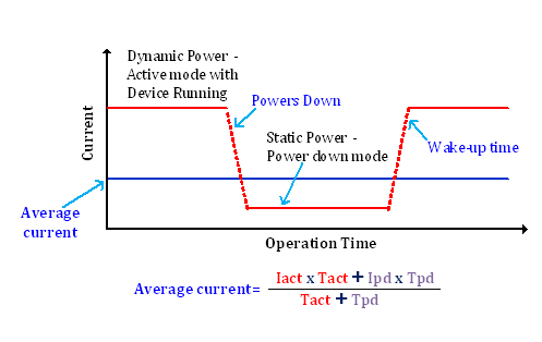
| The overall power consumption of a system, can be defined as: |
| Average Power = Active mode power + Standby/Sleep mode power |
| The average power consumption is the sum of the total energy consumed by the system in Dynamic and Static power modes, divided by the average system loop time. |
|
 |
|
| To improve the battery life it is important to clearly define the Use cases and decide its duration. |
|
| Let us consider one of our OMAP based product design, in which we have categorized multiple power states based on the use cases. Here we shall discuss few use cases to understand the concept better. The main use case of the product is portable Handheld On the Go. The average use of the product is 2 to 3 hours per day. |
|
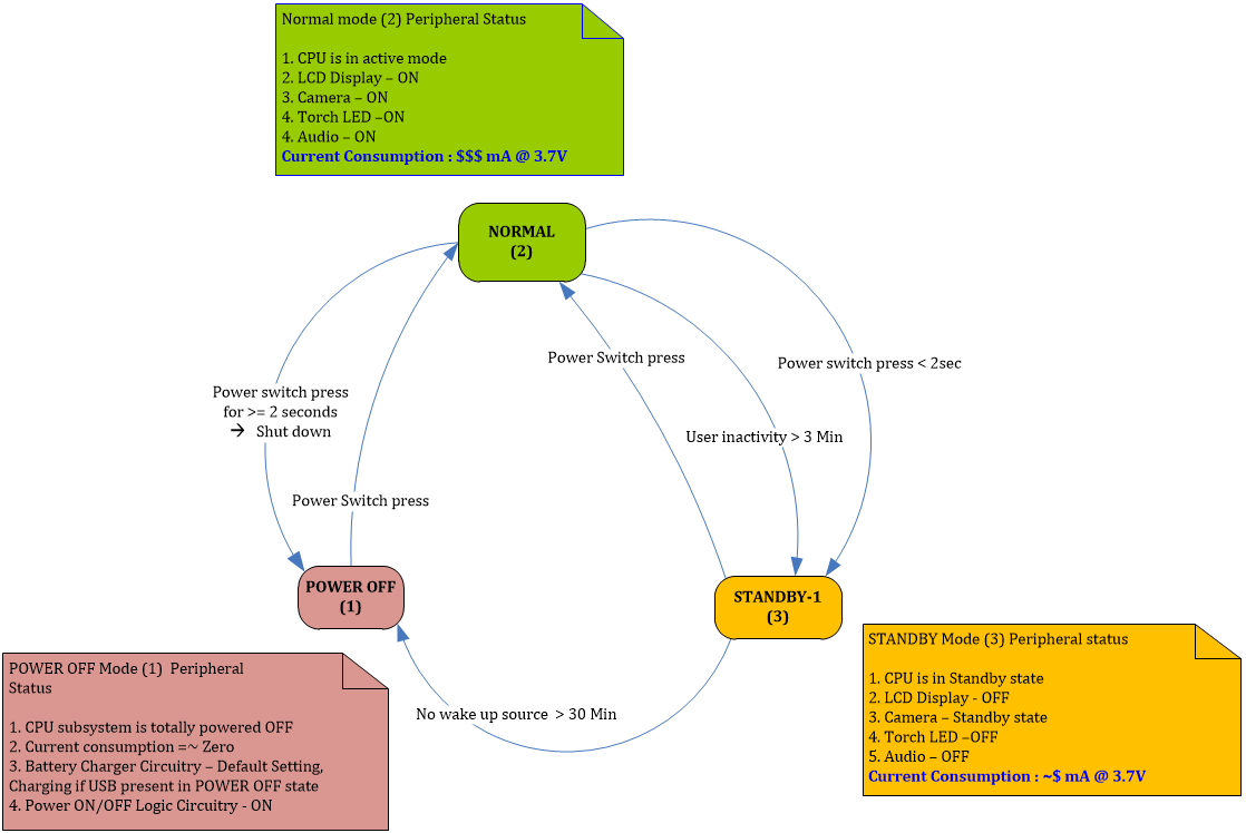
| The product power state divided in to 3, each state and its transition from the states explained in the Power state diagram. |
|
| 1. |
Normal (Active) Mode
|
|
|
| 2. |
STANDBY Mode
|
|
|
| 3. |
Power OFF State
|
|
|
 |
 |
Typical Use Case:
|
|
| The table below defines the typical use case can be used for the power analysis. |
|
|
Mode of Operations
|
Duration of Usage
|
Average Current Consumption in each mode at single-cell (3.7V) Battery
|
Battery Consumption
|
|
Expected Daily Operational Time (Active mode)
|
2 Hours
|
400 mA
|
800 mAH
|
|
Standby state between Active mode
|
4 Hours
|
10 mA
|
40 mAH
|
|
Power OFF State
|
18 Hours
|
1 mA
|
18 mAH
|
|
|
Total Battery consumption per Day
|
858 mAH
|
|
|
How the processor supports power management
|
|
| Let us consider OMAP35xx which supports DVFS as active power management technique. With DVFS, clock rates and voltages are lowered by software based on the performance requirements of the application. For each Operating performance point (OPP), software sends control signals to external regulators in order to set the minimum voltage. In active mode, the OMAP35x supports OPP1, OPP2, OPP3, OPP4 and OPP5. |
|
| With an OMAP35x, DVFS is applicable to two voltage supplies: VDD1 (VDD_MPU_IVA), which supplies the DSP and ARM processors and VDD2 (VDD_CORE), which supplies the interconnects between subsystems and peripherals. These two rails consume most of the chip's power, typically around 75 to 80%. |
|
| For instance, even though the ARM in an OMAP35x processor can run at rates as high as 600 MHz, not all of that computational power is required in every case. The Software can select the OPP mode based on the Use case which reduce/control the processor active mode power consumption. |
|
| In our product normal mode (Live Reading) of operation the OPP5 will be selected to make use of the maximum processor performance and OPP3 used for later viewing the captured images. |
|

|
|
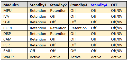
| The static mode also supports four possible power states that depend on power supplied to logic and memory as well as the clocks. These states are active, inactive, retention and off, respectively in decreasing order of power consumption. |
|
| In our product STANDBY mode, the OMAP Standby4 mode selected to achieve the least power consumption. For our product requirement we need to run timer to monitor 30-mins timeout to decide the entry of Power OFF state and few PWM signals for LED indication purpose. The only timer capable of servicing the requirement is GPTimer1 , which is in the wake up power domain of the OMAP. |
|

|
|
| In case of entering Low power mode, it is important to make sure the required Wakeup domain also active. In our product the Power switch connected to OMAP GPIO (GPIO_10) acts Wake-up source. |
|
| In OMAP35x GPIOs wake capability and its corresponding power domain: |
|
| 1. |
When only the WAKEUP power domain is active (ie, OFF mode), only GPIO_1, 9, 10, 11, 30, and 31 can be used to generate a wakeup event. |
|
|
| 2. |
For the rest of the GPIOs in the GPIO1 module (GPIO_0-31, not include the ones above), they can only generate wakeup events if the CORE power domain is active. |
|
|
| 3. |
For GPIOs in modules GPIO2-6 (ie, GPIO_32-191), they can only generate wakeup events if the PER power domain is active. |
|
|
| Our product Power OFF state is typically all the systems block power OFF condition except the Power ON-OFF logic circuit which will monitor the Power switch event. The system will start from reboot once power switch event detected. |
|
 |
How the OS supports power management
|
System and Device power states
|
| The OS (wince) understands the need of the system to be different power requirement states and uses the concept of “Device power state” and "System power state". The windows CE has a power manager which enables applications or device drivers to control their own or the system's power state. The System power state implies a power mode of the whole system and the device-power-state implies a power mode of a particular device/peripheral. While the system power states are numerous and customisable, the device power states are confined to 5 states (D0-D5) with D0 being the most active device power state. It is customisable via registry files as to which power state a device should be in when the system transits from one system power state to another. |
|
Supporting timeouts
|
| The OS enables timeouts between system power states using registry customisable to user requirement. The power manager that maintains the system power states and transitions, maintains timers to check for user activity timeouts so as to enable transition to lower power states. The 3 minutes user inactivity resulting in standby state of the device uses this feature of the OS to reduce power consumption by device on prolonged user inactivity. The power manager provides notification interface for the applications and drivers to know when power management events such as transition to new power state or timeouts occur. |
|
Power State Transition
|
| The power manager provides APIs to set the power state of the system. Once a power state set process is initiated for suspending device, the power manager sets every driver registered with the power manager to the corresponding device state. After the driver power notifications are done with, the power manager enters the OAL code area where some processor level power management activities are done and manages wake up sources before finally putting the processor into idle state to be woken up by one of the wake up sources configured. |
|
OS - OMAP Relation
|
| The OS keeps a tab on the active peripherals under each domain based on the clock request of the peripherals by the OS modules like device drivers. The OS decides the lowest power state possible for each domain based on this activity. When all peripherals are released by the OS modules during standby (i.e. releasing the clock) the OS puts the OMAP into least power state with only the wake-up-domain to be active thereby achieving the least power consumption. |
 |
Tweaks required
|
Clk source enable GPIO
|
| During the least power consumption state, the OMAP works on a 32-KHz clock source rather than the 26MHz clock that is available during active operation. For the OMAP to wake up successfully, the Clock source must be available right after the CPU comes out of idle due to a wake up signal. Enabling the clock source mismatch could cause a device hang. Therefore driving the signal needs to be fine-tuned to the right step of wake up process. |
|
GP Timer for auto-shutoff
|
| With the requirement of 30 minutes of shutoff from standby, the only timer capable of servicing the requirement is GPTimer1 , which is in the wake up domain of the system. Only the GPtimer1 could wake up the device from the low power state. But the same timer was the source for clock synchronisation of the system and the OS. Any change in the timer data would result in a system synchronisation fault and cause a system failure. The timer configuration was done at the final stage of the power flow process where the OS stopped its synchronisation just before the putting the CPU to idle. And right after the processor is out of sleep due to a wakeup signal, the timer is reinstated with exact configuration as to before the sleep. The configuration had to be tested and tweaked for smooth OS run. |
|
Memory Retention
|
| When the OMAP is put to least power state, it is known that register configuration in each modules of CPU is not retained therefore all the configurations need to be redone once out of wake up. The configurations of various peripherals can be taken care in the device drivers but system control registers like power reset and clock control registers do not fall in same category. These registers have to be handled separately and their configuration need to be stored separately before getting into CPU idle and configured back once the CPU is awakened otherwise it could cause a system hang. |
|
Handling race conditions:
|
| During the wake up sequence, when drivers are set back to active power state there may occur a condition in which the peripherals that are used by multiple drivers are accessed out of sync. The race conditions need to be handled such that peripherals cannot be accessed out of sync and other modules should wait till the peripheral accessed by the first intended module is done with its part of work. |
| |