Embedded vision is quickly gaining more prominence in Artificial Intelligence (AI), the Internet of Things (IoT), and other emerging technology based applications. Hence, more companies are looking to cost-efficiently integrate imaging capabilities into their products. For many such products and applications, Mobile Industry Processor Interface (MIPI) is one of the most popular and convenient ways of interfacing cameras with the host processor.
In this blog, we attempt to learn more about the MIPI interface and how MIPI cameras work.
Before we even get into the advantages of the MIPI interface and how MIPI cameras work, let us talk a bit of history on how the interface evolved over time.
Evolution of the MIPI interface
CSI-1
CSI-1 was the original standard MIPI interface architecture that defined the interface between a camera and a host processor.
CSI-2
Released in 2005, the first version of MIPI CSI-2 came with a protocol divided into layers, such as:
- Physical Layer
- Lane Merger Layer
- Low-Level Protocol Layer
- Pixel to Byte Conversion Layer
- Application Layer
Later in 2017, the second version of MIPI CSI-2 was released along with support for RAW-16 and RAW-20 color depths. In addition, it could increase virtual channels from 4 to 32, and reduce Latency Reduction and Transport Efficiency (LRTE).
The third version of MIPI CSI-2 was released in 2019 and came with support for RAW-24 color depth.
CSI-3
MIPI CSI-3 was first released in 2012 followed by the next version in 2014. It provided a high-speed and bidirectional protocol for image and video transmission between cameras and hosts.
Among the three types, MIPI CSI-2 is the most commonly used interface in mobile and remote applications like autonomous driving, drones, smart city, medical imaging, computer vision, etc.
More about MIPI CSI-2
In the previous section, we looked at how the MIPI interface evolved through the years. Now, let us try to understand the MIPI CSI-2 interface a bit more in detail.
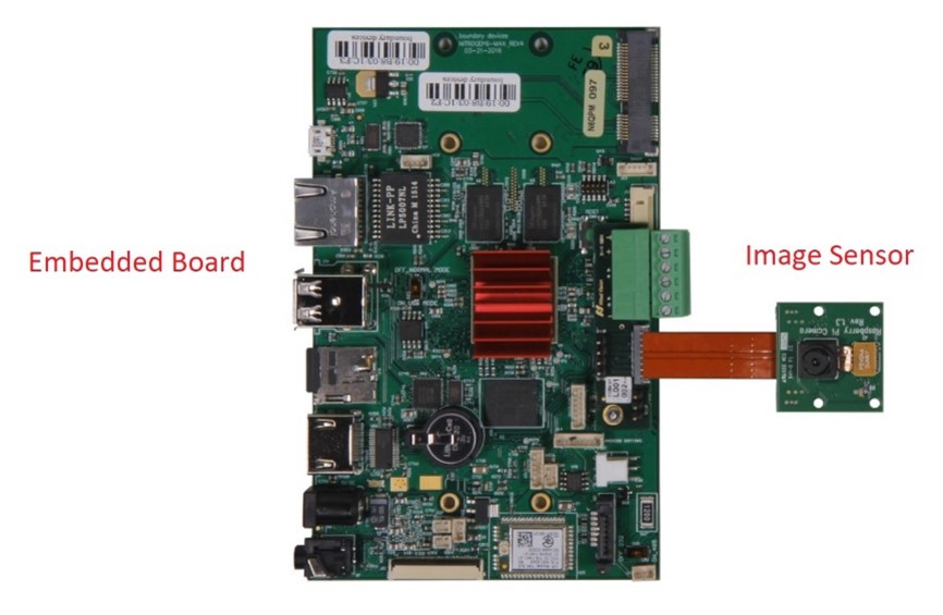
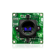
Commonly used in embedded vision systems, MIPI CSI-2 is a camera interface that connects an image sensor with an embedded board to control and process the image data. This helps the sensor and embedded board to act together as a camera system to capture images. The below image represents an embedded camera board connected to an image sensor using a MIPI CSI-2 interface.
MIPI cameras provide higher performance by ensuring better resolution and frame rate than the older parallel interface camera module a.k.a. the Digital Video Port (DVP) interface.
Today, many engineers prefer MIPI CSI-2 cameras over USB cameras. While both cameras come with their own pros and cons, let us look at some of the key advantages of MIPI cameras over USB.
Why MIPI CSI-2 over USB?
In theory, the maximum bandwidth of the USB interface is 5 gigabits per second. Practically, you could attain a bandwidth of about 3.6 gigabits per second.
This limits the ability of vision systems used in many applications to transfer image data fast for various processing and analysis purposes. That is where CSI-2 can be more helpful. It offers a maximum bandwidth of 6 gigabits per second, with an attainable bandwidth of roughly 5 gigabits per second). CSI-2 also makes the process more efficient and faster when compared to the general-purpose interface in USB.
The following image represents the maximum bandwidth supported by the MIPI CSI-2 interface.
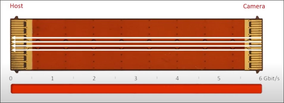
MIPI CSI-2 supports high-performance applications and high-resolution imaging. It can seamlessly transmit images and videos in 1080p, 4K, and 8K formats. It is suited for both single and multi-camera implementations. MIPI CSI-2 also allows larger capabilities for machine awareness across multiple applications.
If you wish to read further on how a MIPI camera compares with a USB camera, have a look at MIPI camera vs USB camera – a detailed comparison. GMSL is also an alternative to MIPI used typically in applications that require image and video data to be transferred to a distance beyond 3 meters. To learn how a GMSL camera is different from a MIPI camera, visit GMSL camera over MIPI camera.
Performance highlights of MIPI CSI-2
Following is a list of key performance highlights of the MIPI CSI-2 interface.
- Its RAW-16 or 24 color depth improves High Dynamic Range (HDR) and Signal to Noise Ratio (SNR), equipping autonomous vehicles with advanced vision capabilities.
- It comes with the ability to use up to 32 virtual channels which accommodates image sensors with multiple data types. This supports multi-exposure and multi-range sensor fusion for Advanced Driver Assistance Systems (ADAS).
- Latency Reduction and Transport Efficiency (LRTE) facilitates real-time perception and optimizes transport to reduce the number of wires and power consumption.
- Differential Pulse Code Modulation (DPCM) compression reduces bandwidth while delivering SNR images devoid of compression artifacts for vision applications.
In general, MIPI cameras are ideal for high-tech OEM embedded vision systems.
Let’s now look at how a MIPI CSI-2 camera works in a vision system.
MIPI Camera: How it works
Typically, the ultra-compact board in a vision system supports MIPI CSI-2 and works with a high range of intelligent sensor solutions. Moreover, it is compatible with many different CPU boards.
MIPI CSI-2 supports the MIPI D-PHY physical layer to communicate to the application processor or System on a Chip (SoC). It can be implemented on either of the two physical layers: MIPI C-PHY℠ v2.0 or MIPI D-PHY℠ v2.5. Therefore, its performance is lane-scalable.
Have a look at the below image to understand the working of a MIPI CSI-2 camera better:

In a MIPI camera, the camera sensor captures and transmits an image to the CSI-2 host. When the image is transmitted, it is placed in the memory as individual frames. Each frame is transmitted through virtual channels. Each channel is then split into lines – transmitted one at a time. Hence, it permits complete image transmission from the same image sensor – but with multiple pixel streams.
MIPI CSI-2 uses packets for communication that include data format and error correction code (ECC) functionality. A single packet travels through the D-PHY layer and then splits into the number of required data lanes. D-PHY operates in high-speed mode and transmits the packet to the receiver through the channel.
Then, the CSI-2 receiver is provided with D-PHY physical layer to extract and decode the packet. The process is repeated frame by frame from the CSI-2 device to the host through an efficient and low-cost implementation.
The MIPI CSI-2 interface makes integration easier and future-proofed. MIPI camera modules can be interfaced with processors such as NXP i.MX8, i.MX7, i.MX6, NVIDIA’s Jetson Nano™, Jetson Xavier™ NX, Jetson AGX Xavier™, Jetson™ TX2, and Jetson™ TX2 NX, and other Linux/Windows/Android-based systems.
If you wish to learn how to choose an interface for your embedded vision system, check out the article How to choose the right interface for an embedded vision system.
e-con’s MIPI Camera Modules
e-con Systems with its 20+ years of experience and expertise in embedded vision has built more than 50 MIPI camera modules that are compatible with all the popular processing platforms. Please have a look at our embedded vision camera portfolio to learn more.
Are you looking for help in integrating the right camera into your product? If yes, please drop a note to camerasolutions@e-consystems.com. Our camera experts will be happy to help you.

Prabu is the Chief Technology Officer and Head of Camera Products at e-con Systems, and comes with a rich experience of more than 15 years in the embedded vision space. He brings to the table a deep knowledge in USB cameras, embedded vision cameras, vision algorithms and FPGAs. He has built 50+ camera solutions spanning various domains such as medical, industrial, agriculture, retail, biometrics, and more. He also comes with expertise in device driver development and BSP development. Currently, Prabu’s focus is to build smart camera solutions that power new age AI based applications.


