

Latency refers to the delay between the moment a camera captures a scene and when that scene is displayed on the viewer’s device. In embedded vision systems, latency is a critical factor—as important as high-resolution imaging. Both directly impact the accuracy and responsiveness of decision-making, which is important in time-sensitive applications such as AI-driven security systems, autonomous vehicles, or automated quality inspection systems.
In this blog, you’ll learn:
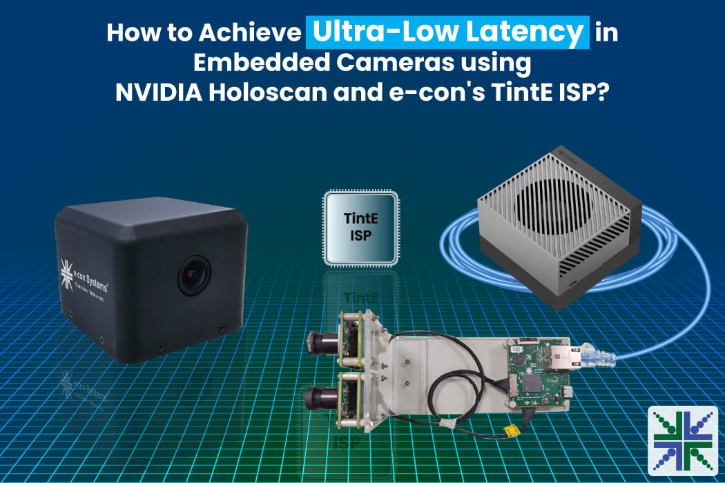
- How to unlock ultra-low latency, as low as 34ms, in embedded vision applications with e-con Systems’ e-CAM85_CUHSB camera integrated with NVIDIA Holoscan Sensor Bridge (HSB)
- How the HSB board processes data using a GPU-based ISP with the Holoscan SDK on the Jetson platform
- How e-con Systems’ TintE™ ISP helps achieve ultra-low latency
- How the HSB board supports Dual Camera Synchronization
You’ll also see a comparison of latency results across different interfaces on the NVIDIA Jetson AGX Orin platform.
About e-con Systems’ e-CAM85_CUHSB
The e-CAM85_CUHSB camera is integrated with the NVIDIA® Holoscan, which leverages Lattice’s FPGA technology and e-con Systems’ TintE ISP and Holoscan Sensor IP on the NVIDIA Jetson Orin platform. This collaborative solution offers broad interface support and high-throughput packetization for AI acceleration on the NVIDIA Jetson AGX Orin platform.
Now, let us first understand what the HSB board is, and then we will delve into its data processing pipeline—both with NVIDIA’s GPU-based ISP and with the TintE ISP.
What is a Holoscan Sensor Bridge – And How Does It Work?
The Holoscan Sensor Bridge provides an FPGA-based interface that uses GPUs to enable low-latency sensor data processing. It incorporates two powerful Lattice FPGAs, each playing a specialized role: CrossLink-NX FPGA handles the reception of high-bandwidth MIPI camera data, while the other CertusPro-NX FPGA is responsible for transmitting this data at speeds of up to thousands of Mbps over 10G SFP+ Ethernet ports.
Its ready-to-use, configurable Holoscan Sensor Bridge IP is paired with the Holoscan software to deliver a sensor-agnostic data-to-Ethernet host platform. This IP simplifies and accelerates FPGA design while offering scalability and configurability to adapt to various sensor-to-host applications.
The board is compatible with the IGX and Jetson AGX Orin platforms through socket-based Ethernet connections. It supports high-speed data transmission via dual 10G SFP+ Ethernet ports for seamless camera integration.
Now, let’s see how it processes data on Jetson using a GPU-based ISP with the Holoscan SDK.
Holoscan Data Processing Pipeline with NVIDIA GPU ISP
The flowchart below illustrates the processing of RAW image data on Jetson using a GPU-based ISP with the Holoscan SDK.
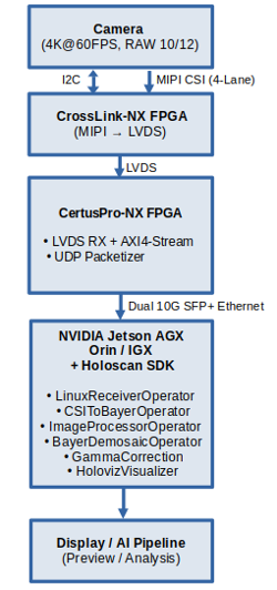 Figure 1: Flowchart of Holoscan Data Processing Pipeline with NVIDIA GPU ISP
This process, as depicted, begins with the e-CAM85_CUHSB camera capturing high-resolution RAW Bayer frames at 4K @ 60FPS or 1080p @ 60FPS with 10/12-bit and transmitting data over a 4-lane MIPI-CSI interface and uses I2C for control. The CrossLink-NX FPGA receives this RAW video via MIPI-CSI and converts it into LVDS format for the next stage of processing. This LVDS data is then sent to the CertusPro-NX FPGA, which decodes it into AXI4-Stream format, packetizes the frame data using UDP, and streams it out through dual 10G SFP+ Ethernet ports.
On the receiving end, the NVIDIA Jetson AGX Orin or IGX, equipped with the Holoscan SDK, captures these packets using the LinuxReceiverOperator.
The NVIDIA Jetson AGX Orin or IGX runs multiple image operations via:
- ImageProcessorOperator
- BayerDemosaicOperator
- GammaCorrection
- HolovizVisualizer
Finally, the processed frames are either displayed on a GUI or forwarded to an AI inference pipeline, making this setup ideal for live previews, object detection, and advanced analytics.
Now, let’s find out how e-con Systems’ TintE ISP—an FPGA-based Image Signal Processor is used with HSB, reducing latency of around 34ms.
Key Advancements in e-CAM85_CUHSB with Holoscan Sensor Bridge
Dual Camera Synchronization using HSB
The HSB supports dual e-CAM85_CUHSB cameras using a hardware trigger called the VSYNC signal. The external VSYNC signal is used as a hardware trigger input for both cameras, ensuring frame-level synchronization.
The detailed diagram below provides an overview of the two e-con cameras connected with the HSB, leveraging Lattice’s FPGA technology and Holoscan Sensor IP on the NVIDIA Jetson Orin platform via a ConnectX-6 Dx NIC.
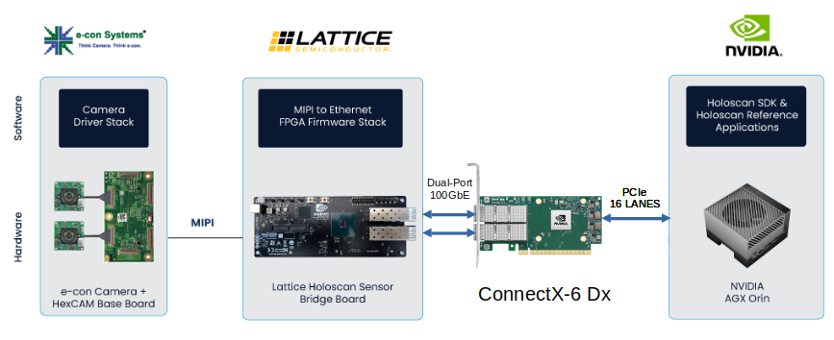
Figure 2: Two e-con Systems’ Cameras connected with HSB
In this dual-camera setup, two e-CAM85_CUHSB cameras are triggered simultaneously using a common VSYNC pulse, ensuring precise frame-level synchronization while streaming at 1080p resolution at 60 fps.
In this two-camera setup, the cameras are simultaneously triggered by the same VSYNC pulse, ensuring that each camera captures frames perfectly in sync and streaming at 1080p resolution @ 60 fps.
The image streams are transmitted over MIPI-CSI to the Holoscan Sensor Bridge, where the CrossLink-NX FPGA converts them to LVDS, and the CertusPro-NX FPGA packetizes and streams the data over dual 10G Ethernet via a ConnectX-6 Dx NIC.
On the receiving side, the NVIDIA AGX Orin platform, running the Holoscan SDK, received the synchronized frame packets for real-time preview and processing.
The image below shows the test results of the latency value measured with the latency meter kit conducted with two cameras connected with HSB, achieving frame-level synchronization.
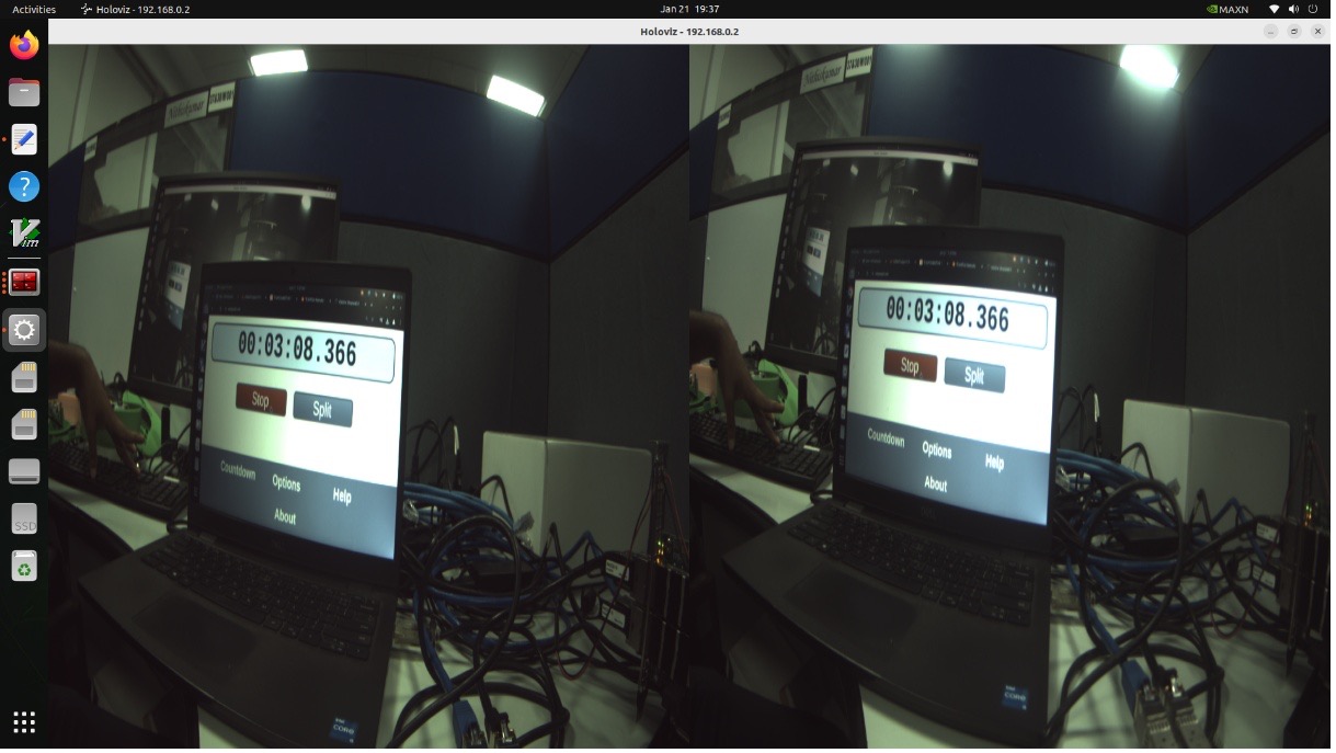
Figure 3: Two Cameras Synchronized Output Image
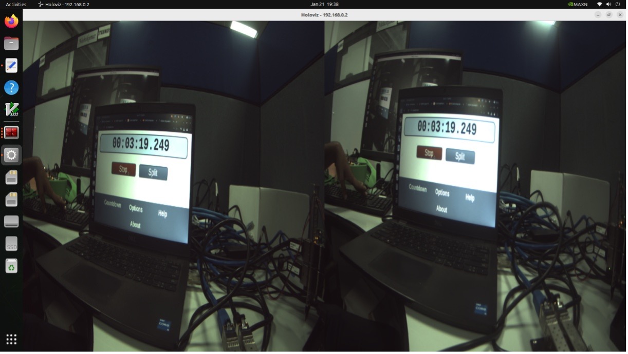 Figure 4: Two Cameras Synchronized Output Image
Achieving Ultra Low Latency with e-con Systems’ TintE ISP
The e-CAM85_CUHSB, a high-resolution camera from e-con Systems, integrates with the NVIDIA Holoscan Sensor Bridge, leveraging TintE ISP, an FPGA-based Image Signal Processor and Lattice’s FPGA for achieving high performance and a low latency of around 34ms.
The flowchart below illustrates the data processing on the Jetson AGX Orin platform using an e-con Systems’ TintE ISP – with the Holoscan SDK.
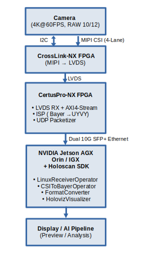
Figure 5: Flowchart of Holoscan Data Processing Pipeline with TintE ISP
The e-CAM85_CUHSB camera connected with HSB performs an initial image stream with a Lattice CrossLink-NX FPGA. The data is then passed to the Lattice CertusPro-NX FPGA, including e-con Systems’ TintE ISP.
The TintE ISP performs key ISP functions such as demosaicing, white balance, color correction, and YUV (UYVY 16-bit) conversion. This enables seamless integration with edge AI platforms like the NVIDIA Jetson AGX Orin and IGX.
Let’s take a closer look at how low latency is achieved at around 34ms in the following section.
Camera Input
The high-resolution e-CAM85_CUHSB camera streams RAW10/12-bit Bayer data over a 4-lane MIPI CSI interface. Sensor parameters such as exposure, gain, resolution, and frame rate are configured via the I2C interface, allowing precise control and synchronization between the image sensor and downstream processing block.
CrossLink-NX FPGA
The incoming MIPI stream is received by the CrossLink-NX FPGA, which performs MIPI D-PHY to LVDS conversion. This step adapts the sensor’s native interface for reliable high-speed transmission to the processing core.
CertusPro-NX FPGA with e-con Systems’ TintE ISP
The CertusPro-NX FPGA serves as the core of the Holoscan Sensor Bridge and integrates three critical components: an LVDS Receiver with an AXI4-Stream Formatter, which prepares incoming video streams for further processing, e-con Systems’ TintE ISP, which performs the complete ISP pipeline, including tasks such as demosaicing, white balance, color correction, and YUV conversion, and UDP Packetizer which converts image frames into high-speed UDP packets.
The block diagram below shows the CertusPro-NX FPGA with the TintE ISP.
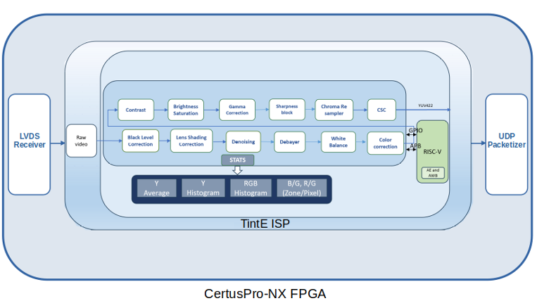
Figure 6: Block Diagram of CertusPro-NX FPGA with TintE ISP
By offloading the ISP workload from the NVIDIA Jetson Platform, the system reduces end-to-end capture latency and maximizes GPU availability for real-time AI inference.
Additionally, e-con Systems customized the Holoscan SDK to enable dynamic runtime control of ISP parameters and support high-resolution still image capture in parallel with live video streaming.
Dual 10G Ethernet
Once image frames are processed and packetized, they are streamed over dual 10G SFP+ Ethernet interfaces, ensuring high bandwidth and low latency for multi-sensor or multi-camera deployments.
Host (NVIDIA Jetson AGX Orin or IGX)
On the host side (Jetson AGX Orin or IGX), the Holoscan SDK takes over using GPU acceleration:
- Linux Receiver Operator: Captures end-of-frame UDP packets to memory.
- CSI to Bayer Operator: Converts CSI-2 embedded RAW data to video frames.
- Format Converter Operator: Resizes and normalizes pixel formats.
- Holoviz Operator: Displays RGB888 data on GUI or feeds it into AI inference.
Now that you have explored how low latency is achieved using TintE ISP, let’s see the advantages of using the TintE ISP.
Benefits of using e-con Systems’ TintE ISP
-
UYVY Conversion with TintE ISP
The TintE ISP converts RAW Bayer data directly into UYVY (16-bit) format on the FPGA. This eliminates the need for additional ISP processing on the host platform, reducing overall latency.
-
Real-Time Image Enhancements
It supports essential real-time enhancements like Auto White Balance (AWB), gamma correction, denoising, lens shading correction (LSC), and color correction (CC). These operations help optimize image quality before it reaches the Jetson platform.
-
Reduced Load on NVIDIA AGX/IGX
By handling the complete ISP pipeline on the FPGA, the TintE ISP significantly reduces the processing load on the NVIDIA Jetson AGX or IGX platform. This frees up valuable GPU resources for AI and computer vision tasks.
-
Dynamic ISP Parameter Control via Holoscan SDK
The TintE ISP fine-tunes ISP parameters such as Contrast, Brightness, Saturation, Sharpness, Auto Exposure (AE) and Auto White Balance (AWB) in real time using the Holoscan SDK.
Let’s now compare its performance with other commonly used camera interfaces.
Interface Comparison: Latency Test Results
This comparison shows that the Holoscan Sensor Bridge consistently delivers lower latency than MIPI and GMSL interfaces, with the lowest latency of 34 ms achieved using e-con Systems’ TintE ISP. By offloading ISP tasks to the FPGA, TintE ISP outperforms traditional GPU-based processing.
| Interface | Sensor | Resolution | Frame rate | ISP | Bits per pixel | Latency (ms) |
| MIPI (Ipex) | IMX715 | 1920 x 1080 | 60 | LibArgus ISP | RAW 10bits |
55ms |
| GMSL | IMX715 | 1920 x 1080 | 60 | LibArgus ISP | RAW 12bits |
50ms |
| Holoscan Sensor Bridge | IMX715 | 1920 x 1080 | 60 | GPU-based ISP | RAW 12bits |
38ms |
| Holoscan Sensor Bridge | IMX715 | 1920 x 1080 | 60 | GPU-based ISP | RAW 10bits |
37ms |
| Holoscan Sensor Bridge | IMX715 | 1920 x 1080 | 60 | e-con Systems’ TintE ISP | UYVY 16bit |
34ms |
Test Setup: How Latency Was Measured
Platform: NVIDIA Jetson AGX Orin platform
Display Output: DisplayPort to HDMI monitor at 1080p60
Camera: e-con Systems’ Holoscan Camera for NVIDIA Platforms featuring IMX715 sensor (used for all interface tests)
Interfaces Tested:
- Native MIPI-CSI (Ipex connector)
- GMSL via serializer-deserializer pair
- Holoscan Sensor Bridge (HSB) via 10G Ethernet (GPU ISP and the TintE ISP)
Frame Format: RAW10, RAW12, and UYVY, depending on the interface and ISP
Software Stack: Holoscan SDK or LibArgus pipeline, depending on the input
The latency is measured using a latency meter kit by Science Mosaic, which measures capture-to-display latency.
This tool generates light pulses and simultaneously detects the emitted signal and the time it appears on the display. It offers millisecond-level accuracy, making it ideal for measuring end-to-end visual latency in embedded vision systems.
e-con Systems Offers Low-Latency Cameras
Since 2003, e-con Systems has been a pioneer in designing, developing, and manufacturing OEM camera solutions. Leveraging our proprietary TintE™ ISP, these camera solutions reduce end-to-end latency while optimizing GPU resources for AI and analytics workloads.
Our portfolio includes a wide range of cameras with features such as multi-synchronization up to 8 cameras, resolutions up to 20MP, HDR with LFM, low-light performance, and support for custom interfaces including GMSL, MIPI, USB, and GigE—customized to meet the demands of diverse embedded vision applications.
To select your custom camera, explore the website at Camera Selector.
For expert guidance on camera integration support, please write to camerasolutions@e-consystems.com.

Prabu is the Chief Technology Officer and Head of Camera Products at e-con Systems, and comes with a rich experience of more than 15 years in the embedded vision space. He brings to the table a deep knowledge in USB cameras, embedded vision cameras, vision algorithms and FPGAs. He has built 50+ camera solutions spanning various domains such as medical, industrial, agriculture, retail, biometrics, and more. He also comes with expertise in device driver development and BSP development. Currently, Prabu’s focus is to build smart camera solutions that power new age AI based applications.